Flachbild-Monochrom- und Niedrigstromanzeigen sind stark auf strukturelle Verpackungen angewiesen, die die Komponenten-Dichte, optische Klarheit und Herstellungskosten ausbalancieren. Unter den primären Integrationsmethoden, die in modernen Elektronik verwendet werden, sticht die COG LCD Screen-Architektur durch ihren Direktmontage-Siliziumansatz hervor. Durch die Eliminierung von Zwischenplatinen und sekundären Verpackungen für Treiber-Integrationsschaltungen (ICs) ermöglicht diese Methode den Hardware-Designern, die Gehäusetiefe zu minimieren und gleichzeitig die Signalintegrität über hochdichte Elektrodenverbindungen zu verbessern.
Das Verständnis der internen Struktur, der Materialinteraktionen, des optischen Verhaltens und der Kommunikationsprotokolle dieser Anzeige-Komponenten ermöglicht es den Designteams, die genauen Anzeigeparameter auszuwählen, die für anspruchsvolle Betriebsumgebungen erforderlich sind.
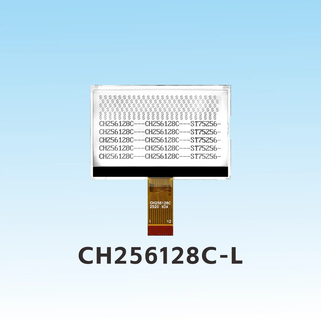
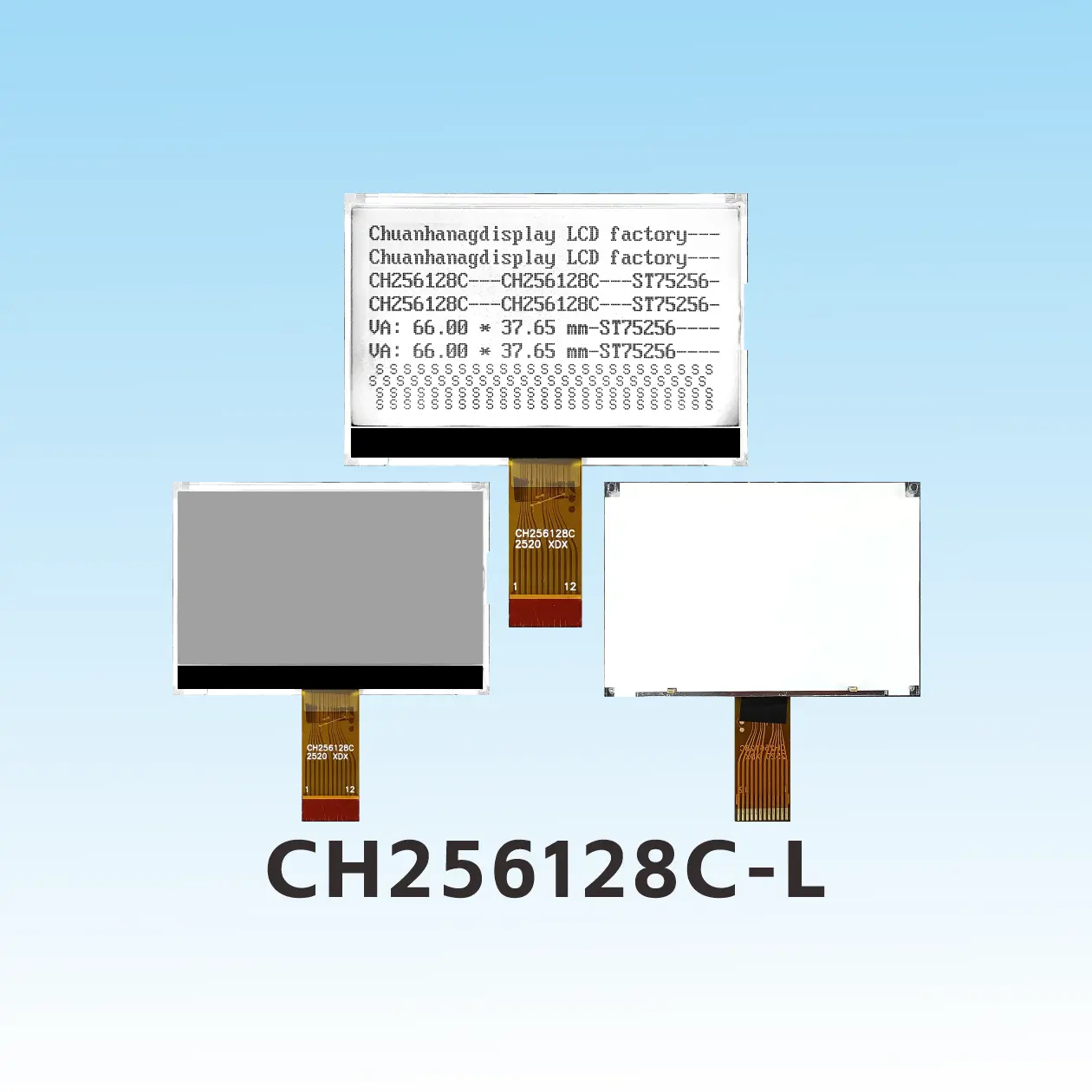
Das definierende Merkmal eines COG LCD Screens ist die Montage des nackten Display-Treiber-Siliziumchips direkt auf die Kontaktkante des unteren Glas- Substrats. Diese Architektur unterscheidet sich deutlich von traditionellen Chip-On-Board (COB) oder Chip-On-Film (COF) Konstruktionen.
Substratzusammensetzung: Das Modul verwendet zwei polierte Float- Glasplatten, typischerweise Soda-Lime oder hochreines Aluminosilikat, mit Dicken zwischen 0,4 mm und 1,1 mm. Das untere Glas reicht über das obere Glas hinaus, um eine Montagekante zu bilden.
ITO-Musterung: Indiumzinnoxid (ITO) wird auf die inneren Glasoberflächen aufgesputtert und fotolithografisch geätzt, um Segmentverbindungen, Matrixanordnungen und Verbindungsfächer zu bilden. Der Blattwiderstand wird streng zwischen 10 Ω/sq und 30 Ω/sq verwaltet, um unerwünschte Spannungsabfälle über lange Anzeigensegmente zu verhindern.
Flüssigkristall-Hohlraum: Der Raum zwischen den beiden Platten, typischerweise zwischen 3 μm und 6 μm über gleichmäßige Silica- oder Polymer-Mikrosphären-Abstandshalter kontrolliert, enthält das Flüssigkristallmaterial, das entlang des Perimeters mit strukturellem Epoxidharz versiegelt ist.
Flexible Leiterplatte (FPC): Anstatt als Träger für das Silizium zu fungieren, dient die FPC in dieser Topologie rein als Brücke zwischen der Systemsteuerplatine und dem Glas-Substrat und enthält passive Leiterbahnen für die Strom- und Logikverteilung.
Die Entfernung des Treiber-IC von einer separaten PCB reduziert die Modul-Dicke um bis zu 60 % im Vergleich zu COB-Modulen. Dies senkt direkt das strukturelle Gewicht und eliminierte die mechanischen Vibrationsanfälligkeiten, die mit verlängerten Lötstiften und schweren Tochterplatinen verbunden sind.
Die direkte Chipmontage erfordert eine elektrische Schnittstelle, die in der Lage ist, feinmaschige Kontaktpads zu handhaben, ohne Kurzschlüsse zwischen benachbarten Kanälen zu verursachen. Dies wird durch anisotropes leitfähiges Film (ACF) Bonden erreicht.
ACF besteht aus einer klebenden Epoxidmatrix, die mit leitfähigen Mikropartikeln imprägniert ist. Diese Partikel sind typischerweise Polymerkugeln, die mit Nickel und Gold beschichtet sind und auf einen engen Durchmesserbereich von 3 μm bis 5 μm ausgelegt sind. Während des thermischen Kompressionsbonding-Prozesses wird der nackte Treiber-IC mit mikrometrischer Präzision über die ITO-Kontaktpads auf dem Glas ausgerichtet. Ein Thermode-Werkzeug wendet kontrollierte Wärme (typischerweise zwischen 180°C und 210°C) und Druck (zwischen 2,0 MPa und 3,5 MPa) für eine Dauer von 10 bis 15 Sekunden an.
Dieser Prozess verformt die leitfähigen Kugeln, die direkt zwischen den Gold Hüben des IC und den ITO-Spuren auf dem Glas eingeklemmt sind, und schafft zuverlässige mikroskopische Leitungsbahnen. Die klebende Matrix füllt die umgebenden Räume und vernetzt sich unter thermischer Aushärtung, wodurch elektrische Isolation entlang der X-Y Ebene gewährleistet wird, während die vertikale Leitung entlang der Z-Achse erhalten bleibt. Fertigungseinrichtungen wie Chuanhang Display setzen strenge optische Inspektionen und Widerstandsüberwachung ein, um sicherzustellen, dass der Kontaktwiderstand über jedem bonded bump unter 1,0 Ω bleibt, während der Isolationswiderstand zwischen benachbarten Anschlüssen 100 MΩ übersteigt.
Die visuelle Leistung eines Displays hängt davon ab, wie die Flüssigkristallflüssigkeit polarisiertes Licht unter variierenden elektrischen Feldern manipuliert. Je nach Zielumgebung können verschiedene Flüssigkristallmodi und Polariserausrichtungen spezifiziert werden.
Twisted Nematic (TN): Verfügt über eine 90-Grad-Molekularverdrehung. Es bietet schnelle Reaktionszeiten und niedrige Betriebsspannungen (typischerweise 3,0V bis 5,0V), was es gut geeignet macht für statische oder niedrig-multiplex Segmentanzeigen mit direkten Betrachtungswinkeln.
Super Twisted Nematic (STN): Verfügt über eine Molekularverdrehung zwischen 180 und 240 Grad. Die steilere elektro-optische Schwellenkurve ermöglicht höhere Multiplexraten (bis zu 1/240 Duty), was komplexe Dot-Matrix Grafiken ohne übermäßiges Ghosting unterstützt.
Film-Compensated STN (FSTN): Integriert einen optischen Retardationsfilm zwischen dem oberen Polarisator und dem Glassubstrat. Diese Schicht neutralisiert die natürliche gelb-grüne oder blaue Hintergrundfärbung des STN-Modus, was hochkontrastreiche schwarze Zeichen auf einem klaren grau-weißen Hintergrund erzeugt.
Double FSTN (DFSTN): Verwendet eine zusätzliche Kompensationsglaszelle anstatt eines passiven Polymerfilms, was zu tiefen, echten schwarzen Hintergründen führt, die für negative Modus-Automobil- und medizinische Displays geeignet sind.
Die Auswahl des Polarisators passt die visuelle Ausgabe weiter an. Reflektierende Polarisatoren verlassen sich vollständig auf Umgebungslicht, was eine unvergleichliche Lesbarkeit bei direkter Sonnenstrahlung und null Hintergrundbeleuchtungsstromverbrauch bietet. Transmissive Polarisatoren benötigen eine kontinuierliche Hintergrundbeleuchtung und glänzen in schwach beleuchteten, hochkontrastierenden dunklen Umgebungen. Transflective Polarisatoren kombinieren eine semi-reflektierende Rückenschicht mit einer aktiven Hintergrundbeleuchtung, die die Lesbarkeit sowohl in völliger Dunkelheit als auch bei direkter Sonnenstrahlung aufrechterhält.
Der Treiber-IC, der an einem COG-LCD-Bildschirm angeschlossen ist, integriert Segment-/Gemeinschaftsverschieberegister, interne Spannungsanhebe-Schaltungen, Temperaturkompensationsnetzwerke und Display-Daten-RAM (DDRAM). Der Host-Prozessor interagiert mit diesen internen Registern unter Verwendung standardisierter Kommunikationsprotokolle.
Serielle Peripherie-Schnittstellen (SPI) Protokolle, die in 3-Draht- oder 4-Draht-Modi konfiguriert sind, minimieren die Pin-Anzahl auf dem Host-Mikrocontroller. Vier-Draht-SPI verwendet dedizierte Leitungen für Chip Select (/CS), Serial Clock (SCL), Serial Data (SDA) und Daten-/Befehlsregisterauswahl (A0 oder D/C), um Übertragungsraten von bis zu 10 MHz bis 20 MHz zu erreichen. Die I2C-Schnittstelle vereinfacht das Routing weiter, indem sie nur zwei Leitungen (SDA und SCL) mit Pull-Up-Widerständen verwendet, die im Standardmodus (100 kHz) oder im Schnellmodus (400 kHz) arbeiten, jedoch bei niedrigeren Bildschirmaktualisierungsraten.
Parallele Schnittstellen (8080-Serie oder 6800-Serie 8-Bit-Busse) bieten maximale Datenübertragungsraten für hochauflösende Punktmatrix-Konfigurationen. Dieser Ansatz ermöglicht schnelle Rahmenaktualisierungen beim Rendern von Mehrrahmenanimationen, schnell wechselnden Messgrafiken oder komplexen Benutzeroberflächen.
Intern erzeugt der Treiber-IC Flüssigkristallansteuerungsspannungen ($V_{LCD}$) unter Verwendung von integrierten Ladungspumpen-Verstärkern, die von einer einzigen $V_{DD}$-Versorgung (typischerweise 1,8V bis 3,3V) betrieben werden. Diese Zwischenbias-Spannungen (von 1/4 bis 1/9 Bias) werden über die Scanning-Gemeinschaftsleitungen und Daten-Segmentleitungen angelegt. Strenge Phaseninversionsalgorithmen (wie Rahmeninversion oder Linieninversion) verhindern, dass Gleichstromspannungsanteile über die Flüssigkristallschicht verweilen, was andernfalls zu elektrochemischer Degradation und permanentem Bildbrand führen würde.
Da der nackte Siliziumchip auf der Glasoberfläche exponiert ist, muss der mechanische und umwelttechnische Schutz direkt in den Modulrand integriert werden.
Ein UV-härtbarer Silikon-Dichtstoff oder struktureller Epoxidharz wird nach der ACF-Bonding über den Rand des Treiber-IC aufgetragen. Dieser schützende Damm schützt die aktive Oberfläche, Bindelinien und feine ITO-Spuren vor atmosphärischer Feuchtigkeit, ionischer Kontamination und physikalischer Abnutzung. Hochwertige Module, die von Chuanhang Display hergestellt werden, halten die strukturelle Integrität über weite Betriebstemperaturbereiche, die von -30 °C bis +80 °C reichen, mit Lagertoleranzen von -40 °C bis +90 °C.
Elektrostatische Entladung (ESD) stellt eine primäre Gefahr für exponierte Glasbaugruppen dar. Da Glas ein elektrischer Isolator ist, können statische Ladungen, die sich auf der Vorderseite ansammeln, durch die niederohmigen ITO-Spuren in die IC-Ausgangspuffer entladen. Eine effektive Systemintegration erfordert leitfähige Gehäuseerdungspunkte, lokalisierte transiente Spannungsschutz (TVS)-Anordnungen auf den FPC-Leitungen und mechanische Dichtungsdesigns, die externe elektrostatische Entladungen vom Glasrand ableiten.
Die Spezifikation einer Anzeigeeinheit für verlängerte industrielle Lebenszyklen erfordert eine systematische Abstimmung zwischen dem physischen Gehäuse, dem elektrischen Leistungsbudget und den optischen Anforderungen.
Sichtrichtung: Definiert relativ zu einem Ziffernblatt. Ein Sichtwinkel von 6:00 Uhr bietet maximalen Kontrast, wenn die Anzeige von unterhalb der normalen Achse betrachtet wird (häufig bei Handmessgeräten und Tischgeräten). Eine Sichtrichtung von 12:00 Uhr zielt auf Geräte ab, die von oberhalb der senkrechten Linie betrachtet werden (wie wandmontierte Thermostate und Rackmontagesysteme).
Hintergrundbeleuchtungskonstruktion: Flache, randbeleuchtete weiße LED-Hintergrundbeleuchtungen verwenden laser-ätiierte Lichtleitplatten (LGP), um eine Helligkeitsuniformität von über 80 % über den aktiven Sichtbereich aufrechtzuerhalten. Strombegrenzende Schaltungen müssen so entworfen werden, dass sie die Vorwärtsspannung ($V_F$) Eigenschaften des LED-Arrays berücksichtigen, während sie innerhalb der thermischen Grenzen bleiben.
Maßgeschneiderte Glasgeometrie: Wenn Standardformate nicht in spezifische Gehäusehüllen passen, ermöglichen maßgeschneiderte Glasprofilierung und benutzerdefinierte ITO-Maskierung die direkte Implementierung spezifischer benutzerdefinierter Symbolsegmente, angepasster aktiver Matrixlayouts und maßgeschneiderter FPC-Ausgangspositionen.
In einem COB (Chip-On-Board)-Modul ist der Treiber-IC direkt auf einer Standard-FR4-Leiterplatte verpackt, die dann mechanisch mit dem LCD-Glas unter Verwendung eines elastomerischen Zebra-Steckverbinders oder eines Heißsiegelverbinders befestigt wird. In einem COG-LCD-Bildschirm wird der Treiber-IC direkt auf das Glassubstrat über ACF gebondet, was die sekundäre Leiterplatte eliminiert, die Modulstärke reduziert und mehrere mechanische Verbindungspunkte entfernt.
Die Viskosität der Flüssigkristalle steigt mit sinkenden Temperaturen, was die molekulare Neuausrichtung verlangsamt und zu längeren Reaktionszeiten führt. Bei höheren Temperaturen können die Durchlasspunkte der Flüssigkristalle die Schwellenspannungen verändern, was den Kontrast des Displays verringert. Treiber-ICs wirken diesen optischen Verschiebungen entgegen, indem sie integrierte Temperatursensoren verwenden, die die Ausgangs-$V_{LCD}$-Steuerkurve dynamisch anpassen, um einen konstanten visuellen Kontrast im Betriebsbereich aufrechtzuerhalten.
Die Wahl zwischen SPI und Parallel hängt hauptsächlich von den verfügbaren I/O-Pins des Mikrocontrollers und den erforderlichen Bildaktualisierungsraten ab. SPI benötigt weniger physische Leitungen (3 bis 4 Pins), was Platz auf der Platine spart und die Routing-Komplexität bei Prozessoren mit niedriger Pinanzahl verringert. Parallele Schnittstellen benötigen 8 bis 12 I/O-Leitungen, ermöglichen jedoch erheblich schnellere Datenübertragungsraten, was sie für große Dot-Matrix-Displays, die Echtzeit-Wellenformdaten aktualisieren, bevorzugt macht.
Ja, die optische Klarheit in Umgebungen mit hoher Helligkeit hängt vom Polarisatormodus ab. Eine reflektierende oder transflektierende Polarisator-Konfiguration reflektiert das Umgebungslicht zurück durch die Flüssigkristallflüssigkeit und bietet einen klaren Kontrast, ohne auszuwaschen. Transflektierende Modelle kombinieren diese Lesbarkeit bei Tageslicht mit einer internen Hintergrundbeleuchtung für die Lesbarkeit bei schwachem Licht.
Das Glasmodul sollte niemals direkten torsionalen oder punktuellen mechanischen Stress von dem äußeren Gehäuse erfahren. Designer sollten Silikon- oder PORON-Schaumelastomerdichtungen zwischen dem vorderen Rahmen, der Glasoberfläche und der unterstützenden Rückplatte integrieren. Dies ermöglicht eine unterschiedliche thermische Ausdehnung zwischen dem Glassubstrat und Kunststoff- oder Metallgehäusen, ohne die Dichtungen des Displays zu beschädigen.
Die Auswahl der optimalen Display-Architektur erfordert eine präzise Koordination der optischen Eigenschaften, elektrischen Antriebsparameter und mechanischen Toleranzen. Chuanhang Display stellt zuverlässige, hochleistungsfähige Display-Module her, die auf präzise Betriebsanforderungen abgestimmt sind, von benutzerdefinierten Segmentlayouts bis hin zu fortschrittlichen Grafiklösungen.
Ingenieurteams können detaillierte Maßzeichnungen, Treiberinitialisierungsquellcode und Validierungsproben anfordern, indem sie sich direkt an unsere Display-Design-Spezialisten wenden.
Kontaktieren Sie das Ingenieurteam von Chuanhang Display:
Anfragen: info@scjhdlcd.com
Benutzerdefinierte Display-Angebote und Musteranfragen: Verfügbar über die Einreichung technischer Anfragen.