Monochrome graphic displays remain a dominant human-machine interface across industrial control units, medical diagnostic instruments, power distribution terminals, and commercial testing devices. Among standard monochrome display formats, the 128x64 dot matrix resolution balances legible information density with low computation overhead on host microcontrollers. Implementing a display unit such as the CH12864 requires an in-depth understanding of silicon controllers, bus interfacing standards, optical configurations, and power rail behaviors to achieve stable performance throughout multi-year equipment lifecycles.
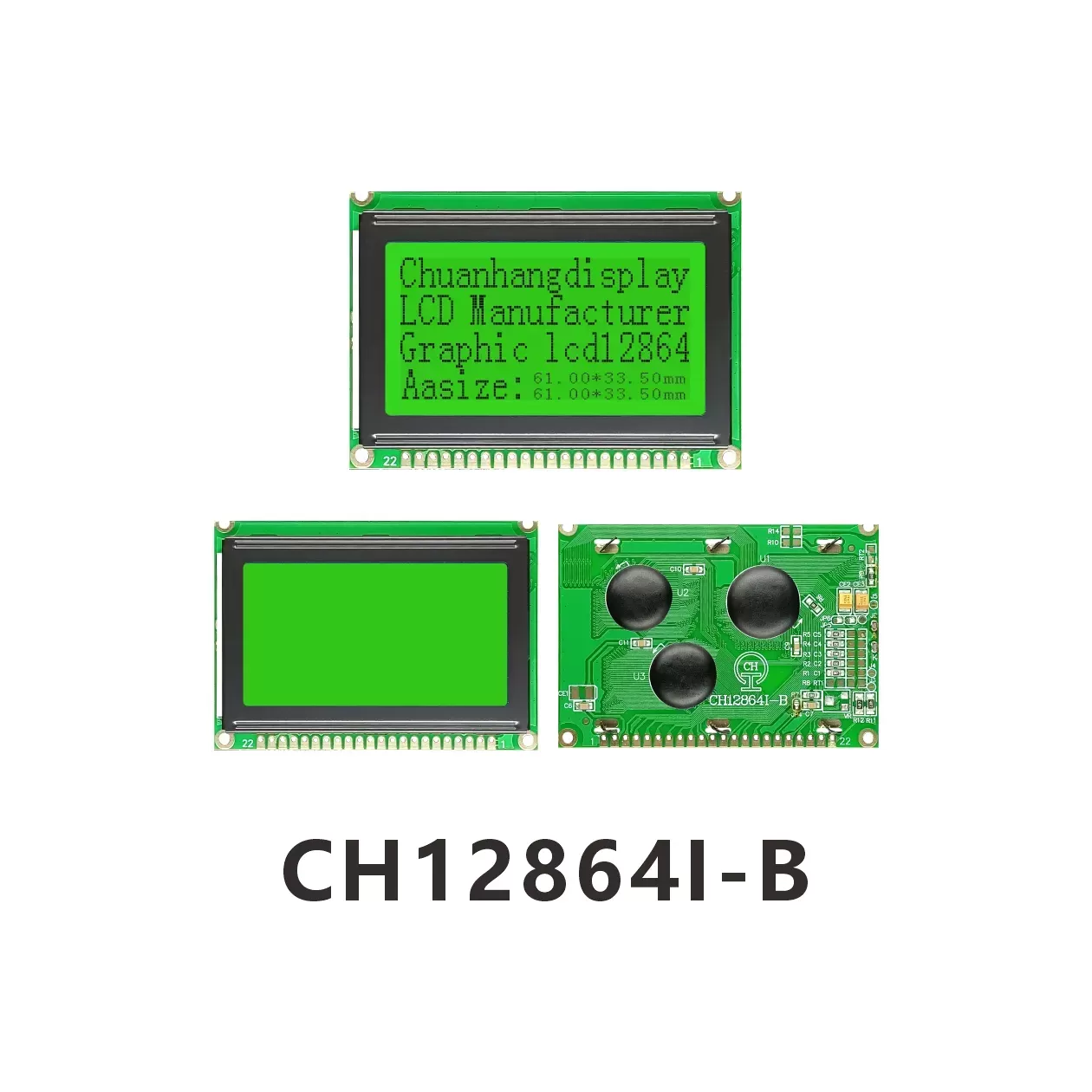
The operational capability of a 128x64 monochrome module depends directly on the integrated driver/controller integrated circuits (ICs) mounted on the printed circuit board (Chip-on-Board, COB) or directly onto the glass substrate (Chip-on-Glass, COG). Modules using the CH12864 platform generally utilize one of three common silicon architectures, each requiring specific memory mapping and firmware handling routines.
Dual-controller configurations, historically based on the KS0108 or compatible architectures like the SBN0064G, divide the 128-column horizontal space into two distinct 64-pixel segments. Each segment is controlled by an independent internal driver IC with its own chip-select line (CS1 and CS2). The display data RAM (DDRAM) inside each controller is organized into 8 vertical pages (Page 0 through Page 7), where each byte represents an 8-pixel vertical column. Writing a full frame requires firmware routines to alternate between CS1 and CS2, setting page addresses and column addresses sequentially from 0 to 63 for each side.
Single-chip controllers featuring built-in font ROMs, such as the ST7920, provide dual operational modes: standard graphic dot matrix mode and alphanumeric text mode containing standard Chinese character sets (GB2312) alongside alphanumeric ASCII tables. In character mode, the host system transmits standard character codes rather than raw pixel bitmaps, substantially reducing host processor load and memory consumption. Graphic mode on the ST7920 utilizes a linear display RAM address space where horizontal lines are addressed directly through vertical and horizontal coordinate registers, streamlining basic geometric drawing routines.
COG-oriented controllers, such as the ST7565 or UC1701, represent a low-power, compact alternative for portable or space-constrained equipment. These controllers operate natively at 3.3V logic levels and incorporate high-efficiency internal DC-DC charge pumps, contrast control registers, and temperature compensation circuits. Memory mapping in these ICs organizes the 64 vertical rows into eight 8-bit horizontal pages that span the entire 128-pixel width continuously, eliminating the need for split chip-select line multiplexing.
Host communication with the CH12864 display module occurs through parallel or synchronous serial protocols. Selecting the proper interface determines the input/output (I/O) pin overhead on the microcontroller, direct memory access (DMA) compatibility, and total frame update throughput.
6800-Series 8-Bit Parallel Interface: Employs an Enable (E) strobe line, a Read/Write (R/W) selection pin, a Register Select (RS / A0) line, and an 8-bit data bus (D0-D7). Data latches on the falling edge of the Enable signal when R/W is low.
8080-Series 8-Bit Parallel Interface: Uses independent Read (/RD) and Write (/WR) active-low strobe signals alongside the Register Select and 8-bit data bus. Write cycles occur on the rising edge of the /WR pulse.
3-Wire and 4-Wire SPI (Serial Peripheral Interface): Relies on Serial Clock (SCLK), Master Output Slave Input (MOSI / SID), Chip Select (/CS), and an optional command/data pin (A0 / RS). Serial transmission significantly conserves GPIO resources on small pin-count microcontrollers, though full-screen redraw rates decrease proportionally with the lower clock speeds.
Bus timing parameters dictate communication reliability. Parallel operations demand strict adherence to enable pulse width requirements (typically 200 ns to 500 ns minimum depending on controller process generation), address setup times before enable assert (minimum 20 ns to 40 ns), and data hold times after enable negation (minimum 10 ns to 20 ns). Violating these timing boundaries under maximum MCU operating frequencies causes intermittent pixel corruption, failed initialization sequences, or dropped command bytes. Interfacing a high-speed ARM Cortex-M or RISC-V processor running above 100 MHz requires insertion of explicit bus wait-states or hardware GPIO delay loops to match the slower response times of the liquid crystal controller ICs.
Operating environment lighting, ambient temperature extremes, and target viewing angles govern the choice of liquid crystal fluid and polarizer type for the CH12864 module.
Nematic fluid chemistry dictates contrast performance, multiplex drive limits, and response times:
STN Yellow-Green (Super Twisted Nematic): Provides a characteristic yellow-green background with dark blue or black pixels. It delivers high contrast under ambient light and functions efficiently with standard yellow-green LED backlights, making it a staple for utility metering and baseline industrial equipment.
STN Blue Negative: Features light-colored translucent pixels against a deep blue background. This mode requires an active backlight to remain visible and is widely specified in indoor instrument clusters and audio-visual monitoring consoles.
FSTN (Film-compensated Super Twisted Nematic): Integrates an optical retardation film to neutralize color dispersion, yielding crisp black characters on a neutral light-gray background (positive mode) or white characters on a true black background (negative mode). FSTN offers higher contrast ratios (often exceeding 8:1) and broader viewing angles than standard STN.
Polarizer configurations establish how the display utilizes external and internal illumination sources. Reflective polarizers rely entirely on ambient light, eliminating backlight power draw, which suits outdoor battery-powered loggers. Transmissive polarizers require a continuous LED backlight to be readable, offering maximum brightness in darkened enclosures. Transflective polarizers combine a semi-reflective backing with high light transmission, maintaining readability in direct sunlight while permitting clear readability in darkness via the integrated LED backlight array.
Viewing direction specifies the angle of maximum contrast relative to the normal plane of the LCD glass. Standard manufacturing formats define either 6 o'clock (bottom view, suitable for displays installed below operator eye level) or 12 o'clock (top view, suited for floor-standing or low-mounted control enclosures). Misalignment between physical installation angle and optical viewing direction results in contrast inversion and unreadable user interfaces.
The liquid crystal fluid requires an internal operating potential (VLCD or V0) that is significantly higher than standard 3.3V or 5.0V logic supplies (VDD). Standard 5V COB iterations of the CH12864 module typically generate this driving voltage through an onboard negative voltage generator (such as a 7660 charge pump IC) to provide a negative potential (VEE) down to -5V or -10V. The net liquid crystal drive voltage, measured as VDD minus V0, generally falls in the range of 8.5V to 10.5V at room temperature for a 1/64 duty cycle display.
Liquid crystal viscosity increases as operating temperatures drop, requiring a higher driving voltage to switch fluid orientation within acceptable frame response windows. Conversely, elevated temperatures thin the fluid, which lowers the threshold voltage needed for molecular reorientation; failing to reduce VLCD under high thermal loads causes background ghosting and severe contrast loss.
Industrial installations subject to wide thermal swings (-20°C to +70°C or extended ranges from -30°C to +80°C) must implement dynamic contrast management. This can be accomplished through external negative temperature coefficient (NTC) thermistor feedback networks in the V0 biasing circuit, or via integrated temperature sensor registers present in advanced display modules from manufacturers like Chuanhang Display. Modulating the driving voltage by approximately -0.05% to -0.1% per degree Celsius ensures stable contrast without manual user adjustment across changing operating climates.
Hardware developers can select between two primary mechanical form factors based on enclosure dimensions, assembly workflows, and vibration profiles.
Chip-on-Board (COB) modules mount the unpackaged driver ICs directly to the rear of a rigid FR-4 PCB, protecting them with cured epoxy glob-tops. The LCD glass connects to the PCB tracks through elastomeric zebra connectors held under mechanical compression by a stamped metal bezel. COB assemblies offer substantial structural rigidity, robust mounting holes at all four corners, simple integration via standard 2.54mm pitch headers, and high resilience against localized thermal stress.
Chip-on-Glass (COG) modules bond the driver silicon directly onto an extended ledge of the liquid crystal glass using anisotropic conductive film (ACF). The interface exits via a flexible printed circuit (FPC) tail. COG configurations eliminate the bulky auxiliary PCB and zebra strips, reducing module thickness to under 2.0mm and lowering overall weight. However, COG glass modules require precise structural support inside the host housing to prevent mechanical bending forces from micro-fracturing the silicon die or peeling the ACF bond.
Backlight design directly influences power consumption and thermal budgeting. Edge-lit LED backlights use minimal LEDs coupled to an acrylic light guide, drawing between 15mA and 45mA, which is appropriate for low-power panels. Bottom-lit (array) backlights place a matrix of discrete surface-mount LEDs directly behind a diffuser layer; these configurations require 100mA to 200mA or more, providing uniform surface luminance above 200 cd/m² for high ambient brightness conditions.
Developing firmware for the CH12864 display module demands structured initialization routines to stabilize internal charge pumps and clear frame buffers before enabling the pixel output. A robust initialization flow follows deterministic states:
Hardware Reset: Drive the hardware reset line (/RST or /RES) low for at least 10 ms after VDD reaches stable operating voltage thresholds, followed by a 10 ms recovery delay before command transmission.
Function Configuration: Transmit commands defining basic bus width (8-bit or 4-bit), basic instruction modes, and graphic display activation bits.
Display Off / Frame Clear: Issue the display-off command to disable optical switching while systematically writing 0x00 to all internal DDRAM memory locations. Clearing memory prevents uninitialized SRAM noise from showing on the screen during startup.
Bias and Duty Setup: Set the correct bias ratio (typically 1/9 bias for 1/64 duty matrix panels) and internal resistor ratio settings if supported by the driver IC.
Display On: Send the display-on command, enable backlight power switching via a host MOSFET, and begin the primary application render loop.
To prevent visual tearing during updates, firmware developers frequently maintain a 1024-byte shadow buffer (128 columns x 64 rows / 8 bits per byte) in MCU internal SRAM. Application graphics—such as line graphs, status icons, and variable text strings—are drawn entirely within this local frame buffer using bitwise operations. Once rendering completes, a background routine or DMA channel flushes the updated buffer to the display memory in a continuous transmission block.
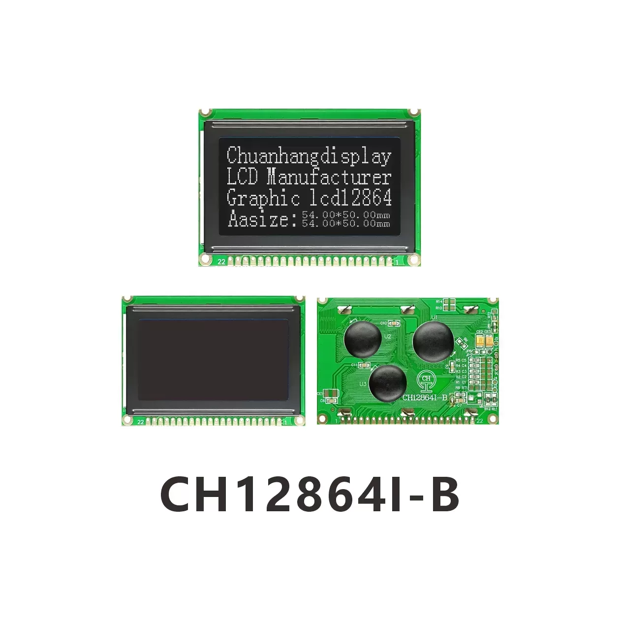
Procuring graphic display hardware for commercial and industrial original equipment manufacturers (OEMs) involves considerations extending beyond base electrical specifications. Production longevity is paramount; industrial controllers frequently remain in serial manufacturing for ten to fifteen years. Working with an established display manufacturer such as Chuanhang Display enables design teams to lock in pinout compatibility, secure silicon availability, and access flexible customization options.
Customization parameters typically include:
Modifying FPC routing, length, connector pitch, or adding stiffeners.
Customizing LED backlight wavelengths, including amber, pure green, or high-CRI white arrays for specific optical filtering requirements.
Integrating resistive (4-wire or 5-wire) or projected capacitive (PCAP) touch overlays with I2C interfaces.
Applying surface treatments such as anti-reflective, anti-glare, or anti-smudge coatings to the outer polarizer.
Mounting temperature compensation circuitry directly onto the carrier PCB.
The ST7920 controller supports both standard graphic dot matrix addressing and built-in Chinese character ROM (GB2312) along with ASCII text modes, communicating over 8-bit parallel or 3-wire/4-wire serial SPI interfaces. In contrast, KS0108-based modules operate exclusively in raw graphic mode via an 8-bit parallel bus split into two separate 64x64 segments, requiring two independent chip-select lines (CS1/CS2) and external font rendering in host software.
Directly driving a 5V module with a 3.3V MCU requires verifying that the logic-high input threshold (VIH) of the display controller is 3.3V compatible (many 5V controllers require VIH to be at least 0.7 * VDD, which equals 3.5V). While outputting from a 3.3V MCU to 5V display inputs often functions if input thresholds allow, reading data back from the display will expose the MCU pins to 5V levels, which will damage non-5V-tolerant GPIOs. Employing bidirectional level shifters or selecting a native 3.3V display variant prevents electrical mismatches.
Ghosting occurs when the liquid crystal threshold voltage decreases as ambient temperatures rise, causing unselected pixels to partially activate. Preventing ghosting requires lowering the liquid crystal drive voltage (V0) proportionally as temperature climbs. This is achieved by incorporating an NTC thermistor into the contrast resistor divider or by programming the internal thermal compensation registers available on modern controllers.
FSTN uses an optical retardation film that provides true black-and-white visual output with significantly higher contrast and wider viewing angles compared to STN. STN is more cost-effective and provides dependable visibility in standard yellow-green or blue formats, but it exhibits lower contrast ratios and noticeable color shifts when viewed off-axis.
Inconsistent initialization typically stems from improper reset timing or noisy supply rails. Ensure that VDD has completely stabilized within specified tolerances before de-asserting the /RST line, and maintain the low pulse on /RST for at least 10 ms to 20 ms. Furthermore, verify that all host GPIO pins are fully configured in the correct output state prior to issuing the first command byte to avoid sending garbage data during power transitions.
Integrating the CH12864 graphic LCD module into industrial equipment requires aligning driver IC architecture, optical parameters, power supply stability, and long-term manufacturing availability. Chuanhang Display engineers and manufactures standard and custom-configured monochrome graphic displays designed to meet exact mechanical, optical, and environmental specifications. Contact our engineering team with your project requirements, target operating parameters, and interface preferences to receive comprehensive technical documentation, evaluation samples, and production quotation support.